1
/
of
1
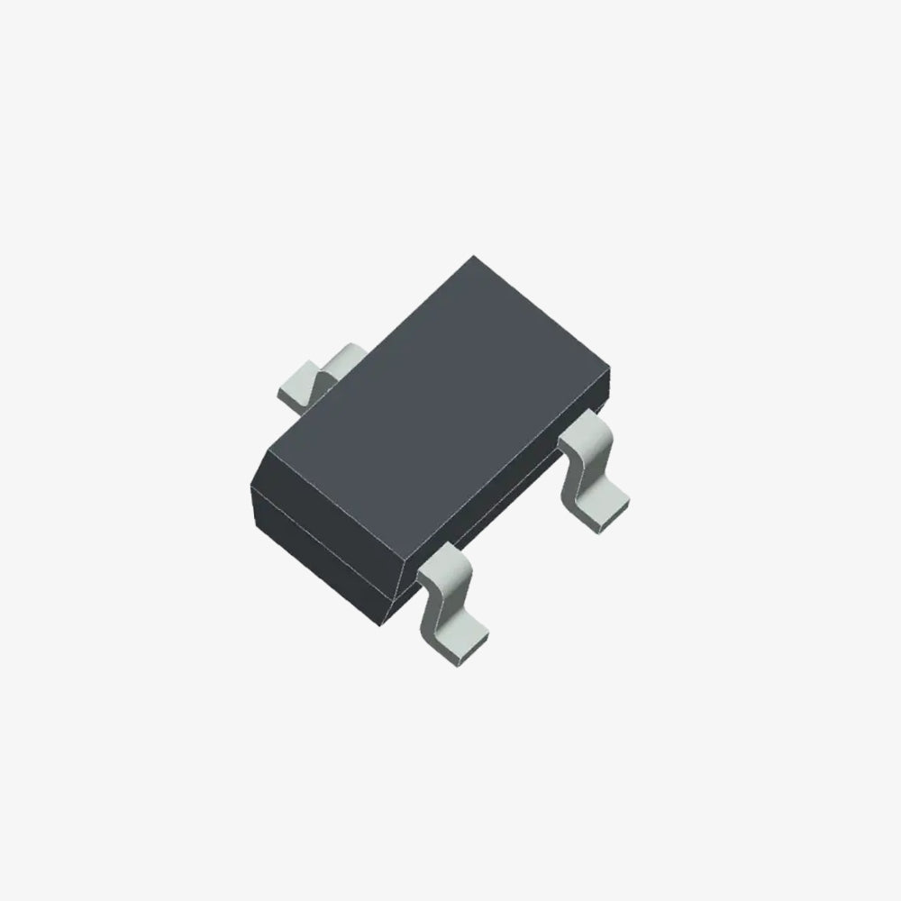
2N7002LT1G N-Channel MOSFET SOT-23 SMD Package
2N7002LT1G N-Channel MOSFET SOT-23 SMD Package
Quantity
10 Pcs MOQ
10 Pcs MOQ
3 Day Global Shipping
Prices are subject to market fluctuations
Prices are subject to market fluctuations
We aim to keep pricing stable, but changes may occur based on external market factors.
Materials and care
Materials and care
HuaQiangBei In-Stock Supply Chain
100% Authentic Products
Rare Chip Sourcing
Share
The 2N7002LT1G is an N-channel MOSFET (Metal-Oxide-Semiconductor Field-Effect Transistor) designed for low-voltage, low-current switching applications. It is housed in a compact SOT-23 surface-mount device (SMD) package, making it ideal for high-density circuit board layouts. Here’s a detailed description of the product:
Key Features:
- Type: N-Channel
- Package: SOT-23 (Surface Mount Device)
- Polarity: N-Channel
- Maximum Drain-Source Voltage (Vds): 60V
- Maximum Continuous Drain Current (Id): 115mA
- Maximum Power Dissipation (Pd): 300mW
- Low On-Resistance (Rds(on)): Typically 7.5Ω at Vgs = 10V
- Gate Threshold Voltage (Vgs(th)): 1V to 2.5V
Applications:
- Load Switching: Ideal for switching low-voltage loads.
- Signal Amplification: Suitable for signal amplification in various electronic circuits.
- Battery-Powered Applications: Commonly used in battery-powered applications due to its low power consumption.
- Low-Power DC-DC Converters: Can be used in DC-DC converter circuits for efficient power conversion.
Physical Dimensions:
- Length: Approximately 2.92mm
- Width: Approximately 1.3mm
- Height: Approximately 1.1mm
Pin Configuration:
- Pin 1 (Gate): The gate terminal, which controls the transistor’s switching.
- Pin 2 (Source): The source terminal, which is typically connected to the negative side of the load.
- Pin 3 (Drain): The drain terminal, through which the main current flows when the transistor is in the 'on' state.
Electrical Characteristics:
- Vds (Drain-Source Voltage): 60V max
- Vgs (Gate-Source Voltage): ±20V max
- Id (Continuous Drain Current): 115mA max
- Ptot (Total Power Dissipation): 300mW max
- Rds(on) (On-Resistance): 7.5Ω typical at Vgs = 10V
- Qg (Total Gate Charge): 2.5nC typical
- td(on) (Turn-On Delay Time): 20ns typical
- td(off) (Turn-Off Delay Time): 50ns typical
Note: Product images are for illustrative purposes only and may differ from the actual product.